Friday, December 27, 2013
Preamplifier for Microphones and Tape Heads


Tuesday, December 24, 2013
Telephone Ring Repeater

Sunday, December 22, 2013
It is the function and feature of cell phone jammer
Then the order of execution of its boot program data read from external memory (font, chip). If not read the information at this time, the CPU internal reset (via the CPU internal "watchdog" or
hardware reset command) bootloader If successful completion of implementation, the CPU was taken from the external font program execution, if acquisition procedures are abnormal, it can lead to a
"watchdog" to reset both the program and from address start. The CPU reads the character through the parallel data and address lines and address lines, together with the read and write control
clock line W / R, some readers may ask, font is how to distinguish between the program read, or read the data? Microcontroller with external program memory chip select signal line or the CS, CE,
and the W / R role, you can allow the character to distinguish between read data or program. Install the main machine of cell phone jammer first.
Phone all the software work processes are carried out under the action of the CPU, the specific division of the five processes described below. These processes are software in the form of data
storage in the phone in EEPROM and FLASHROM of when the phones power supply module detects a power key is pressed, the cell phone battery voltage is converted to a voltage suitable for the use of
the phone circuit value supplied to the power module, the clock circuit supply voltage oscillation signal into the logic circuit, CPU voltage and clock signal, performs the boot process, the first
read from the ROM boot code execution logic The self-test of the system. And all of the reset signal is set high, if the self-test through. cell phone jammer will only act on cell phone
communication.
The CPU is given Watchdog (Watchdog) signal to the module, then the power supply module in the role of watchdog (Watchdog) signal to maintain the boot. Phone is switched on, not only search for the
broadcast control signal Road (BCCH) carrier frequency. Because the system at any time be sent to each user in the community users to broadcast control information. Phone to collect the search to
the strongest (BCCH) carrier frequency. The carrier frequency corresponding to the read frequency correction channel (FCCH), frequency and synchronization of the mobile phone (MS). Each users
mobile phone in different morning (both residential) carrier frequency is fixed, it is to determine when the network by the GSM network operator, rather than determined by the users GSM phone.
Mobile phones to read the sync channel. It is 1 set of main machine of cell phone jammer .
Friday, December 20, 2013
Voltage Tester for Model Batteries


R1,R2 = 47kΩ
R3 = 100kΩ
R4 = 500kΩ
R5 = 1kΩ
R6,R7 = see text (1% resistors!)
R8 = 1kΩ5
R9 = 1kΩ2
R10 = 330Ω
R11 = 15Ω 5W
R12 = 15kΩ
P1 = 100kΩ preset
Capacitors:
C1 = 10nF
C2 = 100nF
Semiconductors:
D1-D10 = LED, red, high effi-ciency
T1 = BC557
T2 = BC517
IC1 = 74HC123
IC2 = LM3914AN
Miscellaneous:
PC1,PC2,PC3 = solder pin
JP1,JP2 = jumper or pushbutton
PCB Layout :

Wednesday, December 18, 2013
MAINS OPERATED CHRISTMAS STAR

Monday, December 16, 2013
High Voltage Pulse Supply Circuit Diagram

Wednesday, October 9, 2013
1 2GHz VCO With Linear Modulation
 For simplicity in the circuit diagram we have shown a potentiometer. The MOD input allows the VCO to be modulated in a digital or analogue fashion, with a transfer slope of –500 kHz/V. In the circuit we have shown an example where MOD is used for frequency shift keying (FSK) modulation. Resistors R1 to R4 shift the level of the data signal so that it has a center value of +1.4 V and an amplitude corresponding to the desired frequency deviation. One example set of values, suitable for use with a 5 V power supply, is as follows: R1 = 480 Ω, R2 = 100 Ω, R3 = 220 Ω und R4 = 270 Ω.
 The input impedance is about 1 kΩ. The output level of the MAX2754 at OUT is around –5dBm into 50 Ω. A coupling capacitor is not required here: the IC already contains one. The MAX2754 is designed for use in transmitters in the 2.4GHz ISM (industrial, scientific and medical) band. This requires the addition of a frequency doubler, which, along with the 2.4GHz antenna, is shown symbolically in the circuit diagram.
Monday, October 7, 2013
Laptop Protector Circuit Diagram

Saturday, October 5, 2013
Car Battery Saver
Prevents the complete discharge of the battery when the door is left open accidentally
I recently forgot to close the door of my car after parking in the garage and I found the battery completely exhausted after the week-end, when I tried to start the engine on Monday morning. This inconvenience prompted me to design a simple circuit, capable of switching-off automatically after a few minutes the inside courtesy lamp, the real culprit for the damage.
 Parts:
R1______________10M 1/4W Resistor
R2______________10K 1/4W Resistor
C1______________47µF 25V Electrolytic Capacitor
IC1____________7555 or TS555CN CMos Timer IC
D1___________1N4148 75V 150mA Diode
Q1____________BD681 100V 4A NPN Darlington Transistor
LP1___________Existing Lamp Bulb, usually 12V 5W
SW1____________SPST Existing Door-Switch
SW2____________SPST Existing Bypass Switch
Circuit operation:
When the door is opened, SW1 closes, the circuit is powered and the lamp is on. C1 starts charging slowly through R1 and when a voltage of 2/3 the supply is reached at pins #2 and #6 of IC1, the internal comparator changes the state of the flip-flop, the voltage at pin #3 falls to zero and the lamp will switch-off. The lamp will remain in the off state as the door is closed and will illuminate only when the door will be opened again. The final result is a three-terminal device in which two terminals are used to connect the circuit in series to the lamp and the existing door-switch. The third terminal is connected to the 12V positive supply.
Notes:
- With the values specified for R1 and C1, the lamp will stay on for about 9 minutes and 30 seconds.
- The time delay can be changed by varying R1 and/or C1 values.
- The circuit can be bypassed by the usually existing switch that allows the interior lamp to illuminate continuously, even when the door is closed: this connection is shown in dotted lines.
- Current drawing when the circuit is off: 150µA.
Thursday, October 3, 2013
Thrifty 2Hz Clock
CMOS circuits are known for their low current consumption. This is particularly important for battery-powered circuits. Unfortunately, oscillators often require quite a bit of current. We therefore propose this oscillator circuit that has a very low current consumption (about 3 µA). The circuit is powered from a type LM334Z current source. The current has been set with R4 to about 3 µA.
Circuit diagram:

Thrifty 2Hz Clock Circuit diagram
This is sufficient to power IC1 and the oscillator circuit around X1. The oscillator generates, with the aid of a cheap watch crystal and a few surrounding parts, a signal that is subsequently applied to the divider in the 4060 and results in a frequency of 2 Hz at pin 3 (output Q13). The level of the output pulses is a lot lower than the nominal 5-V power supply voltage (IC1 is after all powered from a current source with very low current). That is why the signal on pin 3 of IC1 is amplified and inverted by T1. IC3a finally turns it into a proper square wave with acceptably steep edges.
Source : www.extremecircuits.net
Tuesday, October 1, 2013
11 W Stereo or 22 W Mono Power Amp


Sunday, September 29, 2013
HANDY 0 12V DC POWER SUPPLY ELECTRONIC DIAGRAM

For heat protection, heat sink is needed for the BD679 transistor. It is because it will be over tempered when works more than 200mA.
FEATURES:
0v to 12 volt output:
- 700mA with M 2155
- 1.4amp with M 2156
- 1A with 16v AC 1.5 amp plug pack
Friday, September 27, 2013
Push Button Relay Selector
Gate IC1a is connected as a relax-ation oscillator which runs at about 20kHz. Pulses from the oscillator are fed to IC1b, where they are gated with a control signal from IC1c. The result is inverted by IC1d and fed into the clock input (CP0) of IC2. Initially, we assume that the reset switch (S1) has been pressed, which forces a logic high at the O0 output (pin 3) of IC2 and logic lows at all other outputs (O1-O9). As the relay driver transistors (Q1-Q4) are switched by these outputs, none of the relays will be energised after a reset and none of the load devices (speakers, etc) will be selected. Now consider what happens if you press one of the selector switches (S2-S5, etc). For example, pressing S5 connects the O4 output (pin 10) of IC2 to the input (pin 9) of IC1c, pulling it low.
 This causes the output (pin 10) to go high, which in turn pulls the input of IC1b (pin 5) high and allows clock pulses to pass through to decade counter IC2. The 4017B counts up until a high level appears at its O4 output. This high signal is fed via S5 to pin 9 of NAND gate IC1c, which causes its output (pin 10) to go low. This low signal also appears on pin 5 of IC1b, which is then inhibited from passing further clock pulses on its other input (pin 6) through to its output (pin 4), thus halting the counter. So, the counter runs just long enough to make the output connected to the switch that is pressed go high. This sequence repeats regardless of which selector switch you press, so the circuit functions as an electronic interlock system.
Each relay driver circuit is a 2N7000 FET switch with its gate driven from one output of IC2 via a 100W resistor. The relay coil is connected from the drain to the +12V supply rail, with a reverse diode spike suppressor across each coil. If you want visual indication of the selected output, an optional indicator LED and series resistor can be connected across each relay coil, as shown. For selecting pairs of stereo speakers, we’d suggest the use of relays like the Jaycar SY-4052. These operate from 12V and have DPDT contacts rated for 5A. Note that although four selector switches are shown in the circuit, only two relay drivers are shown because of limited space. For a 4-way selector, identical relay drivers would be driven from the O2 and O3 outputs of IC2.
Wednesday, September 25, 2013
A Bedside Lamp Timer Circuit
30 minutes operation, Blinking LED signals 6 last minutes before turn-off
The purpose of this circuit is to power a lamp or other appliance for a given time (30 minutes in this case), and then to turn it off. It is useful when reading at bed by night, turning off the bedside lamp automatically in case the reader falls asleep... After turn-on by P1 pushbutton, the LED illuminates for around 25 minutes, but then it starts to blink for two minutes, stops blinking for two minutes and blinks for another two just before switching the lamp off, thus signaling that the on-time is ending. If the user want to prolong the reading, he/she can earn another half-hour of light by pushing on P1. Turning-off the lamp at users ease is obtained by pushing on P2.
Circuit diagram:
 A Bedside Lamp Timer Circuit Diagram
Parts:
Resistors
R1 = 1K
R2 = 4K7
R3 = 10M
R4 = 1M
R5 = 10K
Capacitors
C1 = 470µF-25V
C2-C4100nF-63V
Semiconductors
C1 = 470µF-25V
C2-C4 = 100nF-63V
D1-D4 = 1N4002
D5 = 5mm. Red LED
IC1 = CD4012
IC2 = CD4060
Q1 = BC328
Q2 = BC547
Miscellaneous
P1,P2 = SPST Pushbuttons
T1 = 9+9 Volt Secondary 1VA Mains transformer
RL1 = 10.5V 470 Ohm Relay with SPDT 2A 220V switch
PL1 = Male Mains plug
SK1 = Female Mains socket
Circuit operation:
Q1 and Q2 form an ALL-ON ALL-OFF circuit that in the off state draws no significant current. P1 starts the circuit, the relay is turned on and the two ICs are powered. The lamp is powered by the relay switch, and IC2 is reset with a positive voltage at pin 12. IC2 starts oscillating at a frequency set by R4 and C4. With the values shown, pin 3 goes high after around 30 minutes, turning off the circuit via C3. During the c6 minutes preceding turn-off.
The LED does a blinking action by connections of IC1 to pins 1, 2 & 15 of IC2. Blinking frequency is provided by IC2 oscillator at pin 9. The two gates of IC1 are wired in parallel to source more current. If required, a piezo sounder can be connected to pins 1 & 14 of IC1. Obviously, timings can be varied changing C4 and/or R4 values.
Source : www.extremecircuits.net
Monday, September 23, 2013
Fuse Box BMW 528I 1982 Diagram
Fuse Box BMW 528I 1982 Diagram


Fuse Panel Layout Diagram Parts: normal speed relay, high speed relay, low beam check relay, high beam relay, low beam relay, fog light relay, main relay, purge valve relay, fuel pump relay, horn relay, wiper control unit, unloader relay.
Saturday, September 21, 2013
Roper 2079b00 Wiring Diagram
 |
| Roper 2079b00 Wiring Diagram |
Wednesday, September 11, 2013
Top Performance LA4446 Stereo Audio Amplifier Circuit
- Low pop noise at power ON/OFF time
- Good ripple rejection: 46dB(typ)
- Good channel separation
- Low residual noise (Rg=0)
- On chip protectors as Thermal protector, Over-voltage/Surge Protector, and pin short protector

Tuesday, September 3, 2013
Mini Drill Speed Regulator Using Voltage Regulator
Mini Drill Speed Regulator Circuit diagram

With the P2 potentiometer can be adjusted the degree of coupling (coupling the output voltage increases with increasing output current). Thus remains constant preset speed. Maximum voltage measured when the P2 is turned up must be about 20% lower than the maximum allowable voltage of the motor (if is not, the value of R1 should be reduced or enlarged accordingly). Voltage regulator is designed with thermal protection, but it must be mounted on a properly dimensioned radiator.
Sunday, September 1, 2013
FM Beacon Broadcast Transmitter 88 108 MHz
Fine frequency adjustment can be made by adjusting the 200 ohm resistor in series with the battery. Oscillator frequency is set by a 5 turn tapped inductor and 13 pF capacitor. The inductor was wound around a #8 X 32 bolt (about 3/16 diameter) and then removed by unscrewing the bolt. The inductor was then streached to about a 3/8 inch length and tapped near the center.
FM Beacon Broadcast Transmitter Circuit Diagram
The ramping waveform at pins 2 and 6 of the timer is applied to the reversed biased diode through a large (1 Meg) resistor so that the capacitance of the diode changes as the ramping voltage changes thus altering the frequency of the tank circuit. Alternately, an audio signal could be applied to the 1 Meg resistor to modulate the oscillator but it may require an additional pullup resistor to reverse bias the diode. The N channel JFET transistors used should be high frequency VHF or UHF types (Radio Shack #276-2062 MPF102) or similar.
Friday, August 16, 2013
Apx280mchannel Power Amplifier Wiring Diagramcircuit Schematic

Subwoofer Wiring Diagram Made Simple.
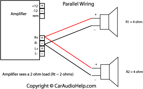
Car Audio Parallel Speaker Wiring Diagram.

Typical 7 Way Trailer Wiring Diagram Circuit Schematic.

Mini Car Subwoofer Amplifier Circuit Diagram Audio Video.

Apx280m 2 Channel Power Amplifier Wiring Diagram Circuit Schematic.
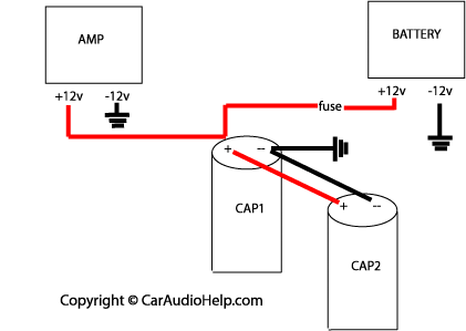
Ideally The Power Capacitor Should Be As Close As Possible.

Subwoofer Wiring Diagrams Understand Ohms Law.

Fuse Box Diagram 1983 Ford Econoline By Janerik.

Subwoofer Wiring Diagram.

Receiver Tv Wiring Diagram Ks3a P Chassis Circuit Schematic.
Wednesday, August 14, 2013
Amplitude Average Detector Circuit
This is a design circuit for sensing amplitude. This circuit is similar peak detector. But the output won’t immediately follow the input peaking. Because the output follows the input peak slowly, averaging effect will be seen at the output. This is the figure of the circuit.

This circuit is work based on two IC’s, there are LM307 and LF351. Use 1% resistor for R1, R2, R3, and R4, and you can achieve negative and positive cycle difference of 0.5dB at the worst case. If you use 5% resistors then the difference between positive and negative cycle gain difference would be about 2dB (worst case). The averaging time constant will depend on R5-C2, you can change to other values if needed. [Circuits diagram source: National Semiconductor Application Notes].
Monday, August 12, 2013
2004 Volkswagen R32 Axle Shaft Joint Diagram

- Axle Assembly
- CV Joints
- Shaft
- Inner Boot
- Outer Boot
Saturday, August 10, 2013
Categorycablewikipedia Free Encyclopedia

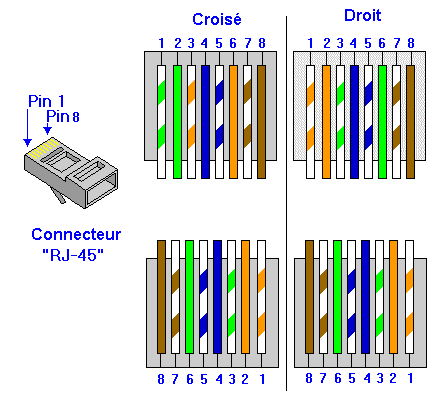
How To Make An Ethernet Cable Cat5 Rj45 Connectors Vsat.

Difference Between Straight Through Crossover And Rollover Cables.

Archon S Site Ethernet Cable Pin Configuration.
Sos Pc Fabrication De C Bles Ethernet Rj45.

Cat5 Network Cable Public Domain Clip Art Image Wpclipart Com.

Figure 3 Tie Eia T568 Ethernet Wiring Standards.

An Ethernet Cable And A Phone Cable.

Cat 5 Ethernet Cable Standards Pin Out Assignments.

Category 5 Cable Wikipedia The Free Encyclopedia.

Limited Ethernet Wiring Diagrams Patch Cables Crossover Cables.
Thursday, August 8, 2013
Boiling Water Reactor BWR Advantages and Disadvantages

1.Reactor pressure vessel 2.Fuel rods 3. Control rod 4.Circulating pump 5.Control rod drive 6.Fresh steam 7. Feedwater 8.High pressure turbine 9.Low pressure turbine 10.Generator 11.Exciter 12.Condenser 13.Cooling water 14.Preheater 15.Feedwater pump 16. Cooling water pump 17.Concrete shield
The above diagram shows BWR and its main parts.The BWR is characterized by two-phase fluid flow (water and steam) in the upper part of the reactor core. Light water (i.e., common distilled water) is the working fluid used to conduct heat away from the nuclear fuel. The water around the fuel elements also "thermalizes" neutrons, i.e., reduces their kinetic energy, which is necessary to improve the probability of fission of fissile fuel. Fissile fuel material, such as the U-235 and Pu-239 isotopes, have large capture cross sections for thermal neutrons.
In a boling water reactor, light water (H2O) plays the role of moderator and coolant, as well. In this case the steam is generted in the reactor it self.As you can see in the diagrm feed water enters the reactor pressure vessel at the bottom and takes up the heat generated due to fission of fuel (fuel rods) and gets converted in to steam.
Part of the water boils away in the reactor pressure vessel, thus a mixture of water and steam leaves the reactor core. The so generated steam directly goes to the turbine, therefore steam and moisture must be separated (water drops in steam can damage the turbine blades). Steam leaving the turbine is condensed in the condenser and then fed back to the reactor after preheating. Water that has not evaporated in the reactor vessel accumulates at the bottom of the vessel and mixes with the pumped back feedwater.
Since boiling in the reactor is allowed, the pressure is lower than that of the PWRs: it is about 60 to 70 bars. The fuel is usually uranium dioxide. Enrichment of the fresh fuel is normally somewhat lower than that in a PWR. The advantage of this type is that - since this type has the simplest construction - the building costs are comparatively low. 22.5% of the total power of presently operating nuclear power plants is given by BWRs.
Feedwater Inside of a BWR reactor pressure vessel (RPV), feedwater enters through nozzles high on the vessel, well above the top of the nuclear fuel assemblies (these nuclear fuel assemblies constitute the "core") but below the water level. The feedwater is pumped into the RPV from the condensers located underneath the low pressure turbines and after going through feedwater heaters that raise its temperature using extraction steam from various turbine stages.
The feedwater enters into the downcomer region and combines with water exiting the water separators. The feedwater subcools the saturated water from the steam separators. This water now flows down the downcomer region, which is separated from the core by a tall shroud.
The water then goes through either jet pumps or internal recirculation pumps that provide additional pumping power (hydraulic head). The water now makes a 180 degree turn and moves up through the lower core plate into the nuclear core where the fuel elements heat the water. When the flow moves out of the core through the upper core plate, about 12 to 15% of the flow by volume is saturated steam.
The heating from the core creates a thermal head that assists the recirculation pumps in recirculating the water inside of the RPV. A BWR can be designed with no recirculation pumps and rely entirely on the thermal head to recirculate the water inside of the RPV. The forced recirculation head from the recirculation pumps is very useful in controlling power, however. The thermal power level is easily varied by simply increasing or decreasing the speed of the recirculation pumps.
The two phase fluid (water and steam) above the core enters the riser area, which is the upper region contained inside of the shroud.
The height of this region may be increased to increase the thermal natural recirculation pumping head. At the top of the riser area is the water separator. By swirling the two phase flow in cyclone separators, the steam is separated and rises upwards towards the steam dryer while the water remains behind and flows horizontally out into the downcomer region. In the downcomer region, it combines with the feedwater flow and the cycle repeats.
The saturated steam that rises above the separator is dried by a chevron dryer structure. The steam then exists the RPV through four main steam lines and goes to the turbine.
Control systems
Reactor power is controlled via two methods: by inserting or withdrawing control rods and by changing the water flow through the reactor core.
Positioning (withdrawing or inserting) control rods is the normal method for controlling power when starting up a BWR. As control rods are withdrawn, neutron absorption decreases in the control material and increases in the fuel, so reactor power increases. As control rods are inserted, neutron absorption increases in the control material and decreases in the fuel, so reactor power decreases. Some early BWRs and the proposed ESBWR designs use only natural ciculation with control rod positioning to control power from zero to 100% because they do not have reactor recirculation systems.
Changing (increasing or decreasing) the flow of water through the core is the normal and convenient method for controlling power.
When operating on the so-called "100% rod line," power may be varied from approximately 70% to 100% of rated power by changing the reactor recirculation system flow by varying the speed of the recirculation pumps. As flow of water through the core is increased, steam bubbles ("voids") are more quickly removed from the core, the amount of liquid water in the core increases, neutron moderation increases, more neutrons are slowed down to be absorbed by the fuel, and reactor power increases. As flow of water through the core is decreased, steam voids remain longer in the core, the amount of liquid water in the core decreases, neutron moderation decreases, fewer neutrons are slowed down to be absorbed by the fuel, and reactor power decreases.
Steam Turbines
Steam produced in the reactor core passes through steam separators and dryer plates above the core and then directly to the turbine, which is part of the reactor circuit. Because the water around the core of a reactor is always contaminated with traces of radionuclides, the turbine must be shielded during normal operation, and radiological protection must be provided during maintenance. The increased cost related to operation and maintenance of a BWR tends to balance the savings due to the simpler design and greater thermal efficiency of a BWR when compared with a PWR. Most of the radioactivity in the water is very short-lived (mostly N-16, with a 7 second half life), so the turbine hall can be entered soon after the reactor is shut down.
Safety Like the pressurized water reactor, the BWR reactor core continues to produce heat from radioactive decay after the fission reactions have stopped, making nuclear meltdown possible in the event that all safety systems have failed and the core does not receive coolant. Also like the pressurized water reactor, a boiling-water reactor has a negative void coefficient, that is, the thermal output decreases as the proportion of steam to liquid water increases inside the reactor. However, unlike a pressurized water reactor which contains no steam in the reactor core, a sudden increase in BWR steam pressure (caused, for example, by a blockage of steam flow from the reactor) will result in a sudden decrease in the proportion of steam to liquid water inside the reactor.
The increased ratio of water to steam will lead to increased neutron moderation, which in turn will cause an increase in the power output of the reactor. Because of this effect in BWRs, operating components and safety systems are designed to ensure that no credible, postulated failure can cause a pressure and power increase that exceeds the safety systems capability to quickly shutdown the reactor before damage to the fuel or to components containing the reactor coolant can occur.
In the event of an emergency that disables all of the safety systems, each reactor is surrounded by a containment building designed to seal off the reactor from the environment.
Comparison with other reactors Light water is ordinary water. In comparison, some other water-cooled reactor types use heavy water. In heavy water, the deuterium isotope of hydrogen replaces the common hydrogen atoms in the water molecules (D2O instead of H2O, molecular weight 20 instead of 18).
The Pressurized Water Reactor (PWR) was the first type of light-water reactor developed because of its application to submarine propulsion. The civilian motivation for the BWR is reducing costs for commercial applications through design simplification and lower pressure components. In naval reactors, BWR designs are used when natural circulation is specified for its quietness. The description of BWRs below describes civilian reactor plants in which the same water used for reactor cooling is also used in the Rankine cycle turbine generators. A Naval BWR is designed like a PWR that has both primary and secondary loops.
In contrast to the pressurized water reactors that utilize a primary and secondary loop, in civilian BWRs the steam going to the turbine that powers the electrical generator is produced in the reactor core rather than in steam generators or heat exchangers. There is just a single circuit in a civilian BWR in which the water is at lower pressure (about 75 times atmospheric pressure) compared to a PWR so that it boils in the core at about 285°C. The reactor is designed to operate with steam comprising 12–15% of the volume of the two-phase coolant flow (the "void fraction") in the top part of the core, resulting in less moderation, lower neutron efficiency and lower power density than in the bottom part of the core. In comparison, there is no significant boiling allowed in a PWR because of the high pressure maintained in its primary loop (about 158 times atmospheric pressure).
Advantages
The reactor vessel and associated components operate at a substantially lower pressure (about 75 times atmospheric pressure) compared to a PWR (about 158 times atmospheric pressure).
Pressure vessel is subject to significantly less irradiation compared to a PWR, and so does not become as brittle with age.
Operates at a lower nuclear fuel temperature.
Fewer components due to no steam generators and no pressurizer vessel. (Older BWRs have external recirculation loops, but even this piping is eliminated in modern BWRs, such as the ABWR.)
Lower risk (probability) of a rupture causing loss of coolant compared to a PWR, and lower risk of a severe accident should such a rupture occur. This is due to fewer pipes, fewer large diameter pipes, fewer welds and no steam generator tubes.
Measuring the water level in the pressure vessel is the same for both normal and emergency operations, which results in easy and intuitive assessment of emergency conditions.
Can operate at lower core power density levels using natural circulation without forced flow.
A BWR may be designed to operate using only natural circulation so that recirculation pumps are eliminated entirely. (The new ESBWR design uses natural circulation.)
Disadvantages
Complex operational calculations for managing the utilization of the nuclear fuel in the fuel elements during power production due to "two phase fluid flow" (water and steam) in the upper part of the core (less of a factor with modern computers). More incore nuclear instrumentation is required.
Much larger pressure vessel than for a PWR of similar power, with correspondingly higher cost. (However, the overall cost is reduced because a modern BWR has no main steam generators and associated piping.)
Contamination of the turbine by fission products.
Shielding and access control around the steam turbine are required during normal operations due to the radiation levels arising from the steam entering directly from the reactor core. Additional precautions are required during turbine maintenance activities compared to a PWR.
Control rods are inserted from below for current BWR designs. There are two available hydraulic power sources that can drive the control rods into the core for a BWR under emergency conditions. There is a dedicated high pressure hydraulic accumulator and also the pressure inside of the reactor pressure vessel available to each control rod. Either the dedicated accumulator (one per rod) or reactor pressure is capable of fully inserting each rod. Most other reactor types use top entry control rods that are held up in the withdrawn position by electromagnets, causing them to fall into the reactor by gravity if power is lost.
Tuesday, August 6, 2013
Circuit Wiring Diagram 1996 Jeep Grand Cherokee Laredo Starting
starting circuit wiring diagrams. This image is clear and easy to read.

Sunday, August 4, 2013
Build 10 Watt Audio Power Amplifier Circuit
